As technology continues to evolve rapidly, so does the demand for more compact, high-performance electronic devices. One of the key innovations that make this possible is the High-Density Interconnect (HDI) PCB. HDI PCBs represent a significant leap forward from conventional printed circuit boards, offering numerous advantages in terms of size, performance, and functionality. But what exactly sets HDI PCB design apart from traditional PCB layouts?
Let’s explore how these two types of PCBs differ and why HDI technology is fast becoming the preferred choice in many advanced electronics applications.
Layer Configuration and Density
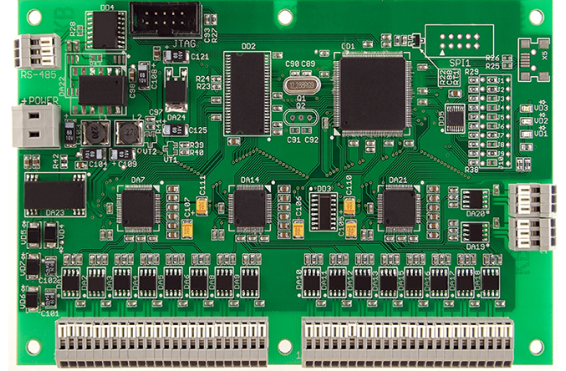
The most striking difference between HDI and conventional PCBs lies in their construction and layer design. While traditional PCBs typically use through-hole vias and are limited in terms of routing density, HDI PCBs incorporate finer lines, smaller vias, and higher wiring density. This allows more functionality to be packed into a smaller space, a feature especially important for modern devices such as smartphones, tablets, and medical equipment.
HDI PCBs often use advanced via technologies such as microvias, blind vias, and buried vias. These allow designers to place more components on both sides of the board without sacrificing performance or reliability. In contrast, conventional PCBs often struggle with limited routing space and are less efficient in utilizing board real estate. Like https://www.pcb-togo.com/
Signal Integrity and Performance
HDI PCB designs also offer superior electrical performance. Because the traces and vias are shorter and more precisely controlled, there is less signal distortion and fewer electromagnetic interference (EMI) issues. This results in better signal integrity, making HDI PCBs an ideal choice for high-frequency and high-speed applications.
In contrast, conventional PCBs—due to their larger via sizes and longer signal paths—can introduce more impedance mismatches and noise into the circuit. For products requiring precision and reliability, HDI technology holds a clear advantage.
Size and Weight Reduction
The push for smaller, lighter devices in the consumer electronics and aerospace industries has made HDI PCB design increasingly important. HDI boards reduce both the size and weight of the final product without compromising functionality. This miniaturization is accomplished through the use of thinner substrates, stacked vias, and tighter component placement.
Conventional PCBs, although more cost-effective for simple designs, cannot match this level of compactness. Their limitations in layer count and component density make them less suitable for applications where space is at a premium.
Design Complexity and Manufacturing
While HDI PCBs offer many advantages, they do come with greater design and manufacturing complexity. Advanced software tools and high-precision equipment are required to handle the tighter tolerances and more intricate layer structures. As a result, the initial cost and design time may be higher compared to standard PCBs.
However, the long-term benefits—such as better performance, enhanced reliability, and the ability to include more features in a smaller footprint—often outweigh these initial challenges.
Applications of HDI Technology
The demand for HDI PCB designs is surging across multiple sectors. Consumer electronics, medical devices, automotive systems, and military-grade technology all benefit from the high performance and miniaturization capabilities of HDI boards. As products continue to shrink while growing in complexity, HDI design is likely to become the industry standard rather than the exception.
To learn more about HDI Printed Circuit Board solutions, visit Pcb-Togo Electronic, Inc.